RAM memory test using no RAM on a COCO 2
Becoming slowly an old man, I like doing retro computing from time to time. Recently I bought an old Tandy Radio Shack TRS-80 COCO 2 that was splendid from the exterior. Unfortunately, when I powered it on, the screen turned green but the BASIC prompt never came up. It took me a while but I was finally able to fix it. The problem was related with the DRAMs. After 30 years, one DRAM chip decided to stop working correctly.
Following video shows what I did, following text describes the same.
The DRAMs are soldered on the board so if you are not sure that the problem is with the DRAM and you know you're not so good at desoldering parts that have been soldered thirty years ago, it takes a lot of courage to decided to attempt to unsolder theses, order new parts and cross your finger the problem was really with them.
To solve that, I decided to write a piece of software that would test the DRAMs without unsoldering them. But how to test the DRAMs... If the DRAM are actually THE problem and you can't dump a software on it to test themselves? One of the solution is to write a special problem that would reside in ROM memory and that will test these DRAMs. By ROM memory I mean remove the "Color Basic" ROM mapped at 0xA000 from the board and replace it momentary will my own ROM with my test program in it.
But the tricky thing is the program has to be written in such manner that it does not require RAM memory. So no variable, no stack, no call to subroutine with BSRs or JSRs. In other words, the program has to rely uniquely on the CPU registers for variable. In the COCO, we're dealing with a 6809 as CPU. This means three 8-bits registers called A, B and DP and four 16-bits registers called X, Y, S and U. The concatenation of the A and B gives the D, but that does not gives a new independant register. Affecting A or B will affect D and vice versa.
As a trick, I could also maybe use registers in external PIAs has possible place to hold some variables or flags but I did not want to do that. Since the program is intended to debug a COCO from which we don't know where the problem is, I wanted to do something that would rely on as less ressource as possible.
In fact, the resources we rely on are:
In fact, the resources we rely on are:
- The 6809 CPU
- The ROM in wich is my test program
- The PIA on which I will make the serial port at 600 bps to send data of the current test via serial port
Writing a program that would not use RAM memory for neither variables or stacks is something I've already done in the past for the company I am working with. At that time, it was with a more powerful CPU, the 68000. With it, we had sixteen 32-bits registers. So it was a little more easy to accomplish something to test RAM without using RAM... Doing something similar with the 6809 is still possible but was less easy. To accomplish that, there are two things that were particularly helpful:
- Use an assembler in which we may use macros
- Use an addressing mode of the 6809 that could mimic a call to a subroutine and return with no stock
For the assembler, I used the open-source asm6809 cross-assembler from this site https://www.6809.org.uk/asm6809/. I chose it because not only it allows to define macros but also because inside the macros we could use labels with conditional branch in it and without causing conflict with many of the same macros in code. Another thing useful with this assembler is that we could also pass parameters to the macro. Finally, we could also invoke another macro within a macro.
Here is an example that combines all these that I use in my RAM TEST program.
Here is an example that combines all these that I use in my RAM TEST program.
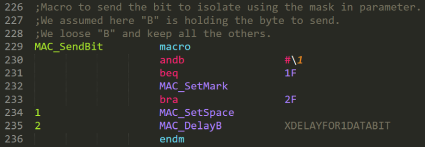
What we see first is its definition generally at the beginning of the code. We see it's called "MAC_SendBit". We check a bit using a mask passed in parameter. We see an example of conditionnal branch with numbered label inside the macro. When giving the suffix "F" like in this example it means to refer to the label "1" going "Forward". So we could also have another label "1" above and to reach it it would be refered as "1B" indicating "Backward". Finally, we see the macro is invoking other macros.
Note: On the "Color Computer 2", there no hardware serial port with silicon shift register... You need to do the serial port yourself using an output pin of a PIA and toggle it yourself with proper timing to gerenate the stream a PC would recognize with start bit, data and stop bit.
Note: On the "Color Computer 2", there no hardware serial port with silicon shift register... You need to do the serial port yourself using an output pin of a PIA and toggle it yourself with proper timing to gerenate the stream a PC would recognize with start bit, data and stop bit.
See here how the macros are invoke later in code.
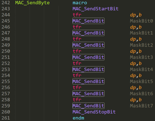
The pertinence of macros in writing a program using no RAM is the fact that since you're not allowed to call routines since there is no stack to indicate the address to come back, it's a little tricky since you cannot write modular code since you cannot nest a series of functional calls. So the way to overcome without manually having to write a lot of code this is by using macros. Having in mind to don't use stack or variables, you may write macros and invoke them in a way that it mimic a little the behavior of calling subroutines. In the above example, when using the macro "MAC_SendBit", it's a little like calling a function "SendBit". When using the macros "MAC_SetMark", "MAC_SetSpace" or "MAC_DelayB", it's a little like also calling functions. But the difference is that you have to take care about the registers you are using to don't lose vital value and you need to be aware that this will take much more code in memory as it's like having unroll the regular nesting calls of routines.
The other trick to work in such condition is to have at least one-level of simili call to subroutine using an adressing mode of the 6809 CPU that allows to jump to the location pointed by a 16-bits registers.
To illustrate that, see the following example used in my RAM test program.
To illustrate that, see the following example used in my RAM test program.
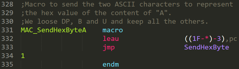
First, in the flow, we arrange thing to have in register "U" the program counter address in which we will need to return after we would virtually call the routine "SendHexByte". The "leau" stands for "Load Effective Address in register U". The term "((1F-*)-3),pc", with that assembler, will compute value of the label 1 forward to where we are and place it in "U". But it's not a JSR or BSR to the "SendHexByte", it's a "jump" and so nothing to push on the stack when doing this.
Then, see the following code for the routine "SendHexByte".
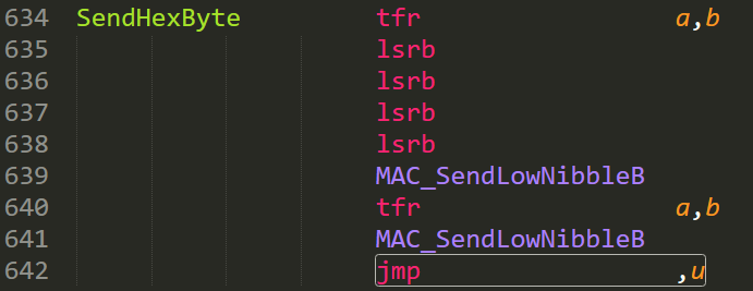
Once we've done our job, instead of having a classic "RTS" for "ReTurn from Subroutine", we do a "JMP ,u" which means we will jump back to our main flow since we've preloaded in "u" the address from where we need to continue the flow of our program. With a 68000, I've already used that technique. I was able to nest also two or three levels of pseudo-call to subroutines this way. But with the 6809, with only 4 registers with 16-bits (the size of the program counter), we cannot nest level of subroutine because we also need the registers for the main job.
Regarding the program itself, my technique to test RAM is simply the result of years of past experiences doing the same at work for boards with 68000 CPU. One thing I learned is that it gives nothing to write and immediately read back the same address immediately after to validate it. In order to dectect trouble it's better to write the entire RAM area with ideally a pseudo random data sequence and then once everything has been filled, re-read back the entire thing and validate if we read back byte for byte the same thing we've writing earlier. If there are errors, we report them and if not, we do again the same thing with different data and so on.
With the Color Computer 2 and my RAM test with no RAM program, I did that. I had a sequence of 353 pseudo numbers with at least once all the values between 0x00 and 0xFF and sequencially filled all over the place the RAM memory and then read back the content to valide it match. Once done, it restarts the sequence with an offset of 1 from the initially 353 values and cycle again with that and so on.
When an error is detected, the application will send via serial port a report like the following.
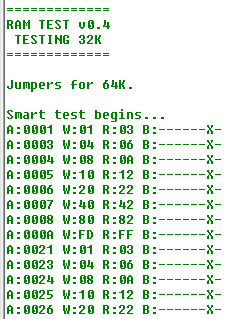
Here, we see many errors. If we look at the first one, we see the address of the error was 0x0001, what was written was 0x01 and what was read back 0x03. To help us to identify the problematic chip we see a code where each character represent the bit d7 to d0. The hyphens indicate bits that were fine and the "X's" indicate the bit with incorrect value. For each of the failed test we see the faulty bit is d1, the bit before the LSB.
In the above example, we visibly have problem with bit d1. then with the schematic of the COCO, we may idenfy from which DRAM chip it is connected to and then determine which one to unsolder and replace. The test program will have saved us the trouble to randomly unsolder and replace DRAM that were fine and not necessary to replace. Directly going to change U14 and that's it.
Before doing the sequence of writing the all the values to all the adresses by cycling in the memory area, my program is doing once a kind of quick smart test of RAM. Instead of writing all over the place, it will write to strategic area strategic values. What I mean by strategic is instead of writing sequencially to all the adresses, it will write few values at adresses like 0x0000, 0x0010, 0x0020, 0x0040, 0x0080, 0x0100, 0x200 and so on where we test addresses with just one address bit set to one at once going up. The idea of doing this is to give quickly an overview of the possible error without having to wait a full linear test to be done. With the error reported at slow speed like 600 bits per second, having a snap shot of the entire memory area tested summarly, that's a plus.
Another point regarding that test program. It could be useful not only because of a defective chip. The initial COCO 2 were delivered with 16K of memory. So someone could have unsolder these chips and replace them with 64K. But, in the process accidentally broke trace on board and so the overall system would not work. With the test program, looking at the result closely, it might help to figure at which chip or close to which ones the traces have been cut in the manipulation.
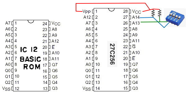
To store the binary image result to an EPROM, it is hardly possible to find today a 24-pins with the same pinout as the one the COLOR BASIC ROM of the COCO. So some work has to be done. I finally used a 27C256 which is a 32K, so 4 times larger than the 8K chip to replace. But instead of waiting this space, here is what I did: on my small prototype I added a pack of dip switches to control the two upper address lines to allow me to do a kind of bank switching manually with the dip switches. The pseudo schematic looks like the following:
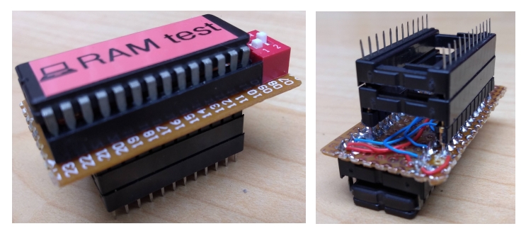
So it allowed me to store in memory four different applications. I stored the following:
- Nothing, spare block
- My test program for 32K
- My test program for 16K
- The actual Microsoft COLOR BASIC ROM content
Once completed, my special piggy back socket montage looks like the following:
Link for download
So that's it. Here follows the pertinent files.
- Source code in assembly of my RAMTEST using no RAM
- Binary image for 16K RAMTEST
- Binary image for 32K RAMTEST
- Binary image of what I stored in a 27C256 EPROM which include COLOR BASIC, 16K RAMTEST and 32K RAMTEST
- Link to my YouTube video on this